|
|
|
|
||||||||||||||||||||
|
||||||||||||||||||||
|
|
||||||||||||||||||||
|
|
|
|
|||
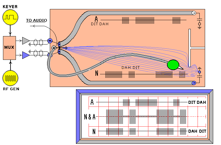
| DEMO: The
Demo is of a resonant Groundplane where a second
Groundplane (or Shield) in brought into proximity,
and the effect on its resonate frequency. |
|||
 |
|||
|
|||
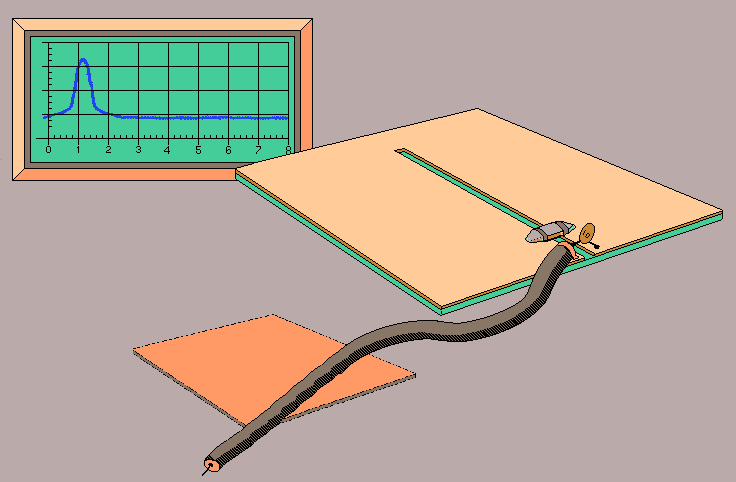
| This "Resonant Groundplane" demo is a simple example of what
can be a very complex problem; i.e., a non-homogeneous groundplane (many
apertures) with many different return currents from many different devices
running at various rates; having rise and fall times from a few nanoseconds,
to fractions of a nanosecond--all sharing the Groundplane as their return
paths.
This can gives rise to device oscillations and instabilities, generating NOISE and Crosstalk, etc. This effect is due to the imperfect "A.C. grounding of active devices, and the many parasitic reactances that inhabit the circuit & board topology. This complex environment could, I suppose, be analyzed and the "tuned circuits" identified... --you get the idea. To make the point that the use of GOOD Groundplane Design is important, especially in a mixed environment (analog/digital), an experiment that I call a "resonant groundplane" was designed. In the example, a 4" X 6" copper clad board was used, and a narrow (1/8") strip of the copper cladding was peeled almost the length of the board, such that, electrically it looked like the letter "U." At the edge of the board where the peeling began, a capacitor was soldered, bridging the planes on both sides of the narrow GAP. Then both sides are driven (the capacitor is shunting) with a loosely coupled signal sweep generator and adjusted until the resonance is found. The display presentation is of a swept network having a definite resonance. Then a separate homogeneous groundplane brought into close proximity, which causes the resonant frequency to increase in frequency, as well as, the "Q" of the resonance to diminish. The implication in all this is that a GOOD groundplane design has as few APERTURES as is practicable. And where apertures are unavoidable, than shielding or a secondary parasitic groundplane can ameliorate the problems. |
|||
| Shielding | ||
| Shielding can be anything from using a coaxial or shielded cable, to a sealed conductive chamber for circuit isolation. Shielding serves a reciprocal purpose: it protects the circuit it is shielding from outside noise or unwanted signals; and conversely, it contains its own signals and thus protects the outside world from interference of its own making. Shielding is mostly used to block electrostatic or "E" fields (Faraday shield). However, if ferrous metal (tempered Mu Metal works best for magnetic fields) is used, then both electrostatic and some level of magnetic shielding is accomplished. This is especially useful where open frame transformers or unshielded coils are used and would otherwise exchange signals by mutual inductance. | ||
|
||
|
|
||
| One important requirement for a shield to be effective, is that there must be no currents flowing through the shield itself. This is best accomplished by connecting the reference or common, at only one point on the shield, thus preventing any flow of current. The reason for this, is that any current flowing in the shield material itself can produce secondary fields on the other side of the shielding material and thereby reducing the effectiveness of the shield. An extreme case of this might be a shielded cable, whose shield has a different potential at each end, and the resulting current flow in the shield, inducing unwanted noise into the center or shielded conductors. (In this situation one might find a remedy by disconnecting one or the other ends of the cable's shield. However, this may not prove satisfactory in certain environments, and may require a "Guard" potential, or better still: Optical Isolation) | ||
|
|
||
| There is an active form of shielding where fields of counter EMF (equal
but opposite) are generated to cancel out the offending fields. A good
and simple example of this is the AC power transformer, where a "shorted
turn" is used to generate a nulling field.
The shorted turn, is a seamless band of copper that wraps the transformer core in one direction. When cut by the rising and collapsing magnetic flux -- caused by the transformer action -- the shorted turn acts as a very low impedance, high current secondary winding, and generates a counter EMF, and because this winding is shorted, it generates a rising and collapsing magnetic field of opposite polarity thereby nulling the original stray magnetic flux. In some cases of severe common mode noise, the shield can be made to carry an equal but opposite noise current to counter the interfering noise. However, this is not for the faint-of-heart: any slight change of the mechanical or electrical parameters, and the cancelling noise becomes the noise noise! |
||